ddr2_usr_be.ddr2_usr_be_arc Architecture Reference
top module of DDR2 RAM controller More...
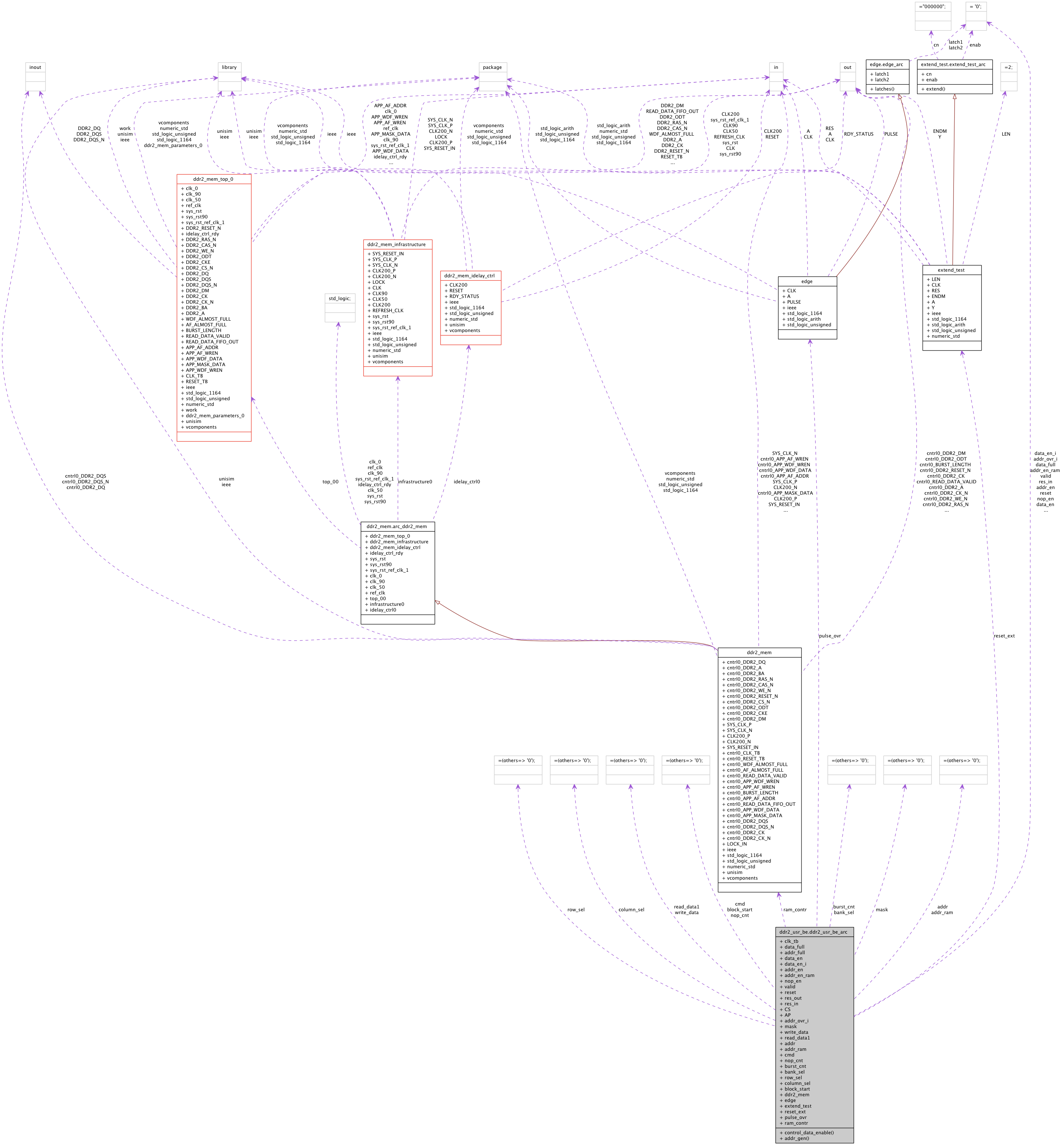
Inheritance diagram for ddr2_usr_be.ddr2_usr_be_arc:

Collaboration diagram for ddr2_usr_be.ddr2_usr_be_arc:
Processes | |
| control_data_enable | ( clk_tb ) |
| data enable control | |
| addr_gen | ( clk_tb ) |
| address generation | |
Components | |
| ddr2_mem | <Entity ddr2_mem> |
| RAM controller. | |
| edge | <Entity edge> |
| Edge detection. | |
| extend_test | <Entity extend_test> |
| pulse extender | |
Signals | |
| clk_tb | std_logic := ' 0 ' |
| data_full | std_logic := ' 0 ' |
| addr_full | std_logic := ' 0 ' |
| data_en | std_logic := ' 0 ' |
| data_en_i | std_logic := ' 0 ' |
| addr_en | std_logic := ' 0 ' |
| addr_en_ram | std_logic := ' 0 ' |
| nop_en | std_logic := ' 0 ' |
| valid | std_logic := ' 0 ' |
| reset | std_logic := ' 0 ' |
| res_out | std_logic := ' 0 ' |
| res_in | std_logic := ' 0 ' |
| CS | std_logic := ' 0 ' |
| AP | std_logic := ' 0 ' |
| addr_ovr_i | std_logic := ' 0 ' |
| mask | std_logic_vector ( 15 downto 0 ) := ( others = > ' 0 ' ) |
| write_data | std_logic_vector ( 127 downto 0 ) := ( others = > ' 0 ' ) |
| read_data1 | std_logic_vector ( 127 downto 0 ) := ( others = > ' 0 ' ) |
| addr | std_logic_vector ( 35 downto 0 ) := ( others = > ' 0 ' ) |
| addr_ram | std_logic_vector ( 35 downto 0 ) := ( others = > ' 0 ' ) |
| cmd | std_logic_vector ( 2 downto 0 ) := ( others = > ' 0 ' ) |
| nop_cnt | std_logic_vector ( 2 downto 0 ) := ( others = > ' 0 ' ) |
| burst_cnt | std_logic_vector ( 1 downto 0 ) := ( others = > ' 0 ' ) |
| bank_sel | std_logic_vector ( 1 downto 0 ) := ( others = > ' 0 ' ) |
| row_sel | std_logic_vector ( 12 downto 0 ) := ( others = > ' 0 ' ) |
| column_sel | std_logic_vector ( 6 downto 0 ) := ( others = > ' 0 ' ) |
| block_start | std_logic_vector ( 2 downto 0 ) := ( others = > ' 0 ' ) |
Component Instantiations | |
| reset_ext | extend_test <Entity extend_test> |
| extend reset from ram controller | |
| pulse_ovr | edge <Entity edge> |
| make overflow flag 1 cycle | |
| ram_contr | ddr2_mem <Entity ddr2_mem> |
| RAM controller. | |
Detailed Description
top module of DDR2 RAM controllerInterface to DDR2 RAM controller, generates addresses, takes care of access scheme (burst mode, pauses, ...)
Definition at line 79 of file ddr2_usr_be.vhd.
Member Function Documentation
| addr_gen | ( clk_tb ) |
address generation
Definition at line 241 of file ddr2_usr_be.vhd.
00241   addr_gen : process(clk_tb)
00242   begin
00243     if clk_tb'event and clk_tb = '1' then
00244
00245       if (reset or ADDR_RES) = '1' then
00246         column_sel  <= (others => '0');
00247         bank_sel    <= (others => '0');
00248         row_sel     <= (others => '0');
00249         burst_cnt   <= "00";
00250         nop_cnt     <= (others => '0');
00251         addr_en_ram <= '0';
00252         nop_en      <= '0';
00253
00254       elsif addr_full = '0' and EN = '1' then
00255 -- elsif stop_write = '0' then
00256
00257         if R_W = '0' and data_full = '0' then  -- 7+1 write burst structure
00258
00259           burst_cnt <= burst_cnt + 1;
00260           --addr_en <= '1';
00261           --nop_en <= '0';
00262
00263           if burst_cnt = "11" then
00264             if nop_en = '1' then
00265               addr_en_ram <= '0';
00266             else
00267               addr_en_ram <= '1';
00268             end if;
00269             nop_cnt <= nop_cnt + 1;
00270           else
00271             addr_en_ram <= '0';
00272             nop_cnt     <= nop_cnt;
00273           end if;
00274
00275           if burst_cnt = "10" then
00276             if nop_cnt = "111" then
00277               nop_en     <= '1';
00278               bank_sel   <= bank_sel;
00279               column_sel <= column_sel;
00280               row_sel    <= row_sel;
00281             else
00282               nop_en <= '0';
00283             end if;
00284           end if;
00285           if nop_en = '0' then
00286             if burst_cnt = "11" then
00287               column_sel <= column_sel + 1;
00288               if column_sel = "1111111" then
00289                 bank_sel   <= bank_sel + 1;
00290                 column_sel <= (others => '0');
00291                 if bank_sel = "11" then
00292                   row_sel  <= row_sel + 1;
00293                   bank_sel <= "00";
00294
00295                   if row_sel = "1111111111111" then
00296                     nop_cnt <= (others => '0');
00297                     nop_en  <= '0';
00298                   else
00299                   end if;
00300
00301                 else
00302                   row_sel <= row_sel;
00303                 end if;
00304               else
00305                 bank_sel <= bank_sel;
00306               end if;
00307             else
00308               column_sel <= column_sel;
00309             end if;
00310           end if;
00311
00312         else                            -- 1+1 read structure
00313
00314           burst_cnt <= burst_cnt + 1;
00315
00316           if burst_cnt = "11" then
00317             if nop_en = '1' then
00318               addr_en_ram <= '0';
00319             else
00320               addr_en_ram <= '1';
00321             end if;
00322             nop_en <= not nop_en;
00323           else
00324             addr_en_ram <= '0';
00325             nop_cnt     <= nop_cnt;
00326           end if;
00327
00328           if nop_en = '0' then
00329             if burst_cnt = "11" then
00330               column_sel <= column_sel + 1;
00331               if column_sel = "1111111" then
00332                 bank_sel   <= bank_sel + 1;
00333                 column_sel <= (others => '0');
00334                 if bank_sel = "11" then
00335                   row_sel  <= row_sel + 1;
00336                   bank_sel <= "00";
00337
00338                   if row_sel = "1111111111111" then
00339                     nop_cnt <= (others => '0');
00340                     nop_en  <= '0';
00341                   else
00342                   end if;
00343
00344                 else
00345                   row_sel <= row_sel;
00346                 end if;
00347               else
00348                 bank_sel <= bank_sel;
00349               end if;
00350             else
00351               column_sel <= column_sel;
00352             end if;
00353           end if;
00354
00355         end if;
00356
00357       elsif R_W = '0' and EN = '0' then
00358         addr_en_ram <= '0';
00359         nop_en      <= '0';
00360         nop_cnt     <= (others => '0');
00361
00362       else
00363
00364         addr_en_ram <= '0';
00365         burst_cnt   <= burst_cnt;
00366
00367       end if;
00368     end if;
00369   end process addr_gen;
| control_data_enable | ( clk_tb ) |
data enable control
Definition at line 220 of file ddr2_usr_be.vhd.
00220   control_data_enable : process(clk_tb)
00221   begin
00222     if clk_tb'event and clk_tb = '1' then
00223       data_en <= data_en_i;
00224       if reset = '1' then
00225         data_en_i <= '0';
00226       else
00227         if R_W = '0' and data_full = '0' and nop_en = '0' and EN = '1' then
00228           --if R_W = '0' and stop_write = '0' and nop_en = '0' then
00229           data_en_i <= '1';
00230         else
00231           data_en_i <= '0';
00232         end if;
00233       end if;
00234     end if;
00235   end process;
Member Data Documentation
ddr2_mem [Component] |
edge [Component] |
extend_test [Component] |
reset_ext extend_test [Component Instantiation] |
The documentation for this class was generated from the following file: