ddr2_mem_infrastructure.arc_infrastructure Architecture Reference
Services for DDR2 memory controller. More...
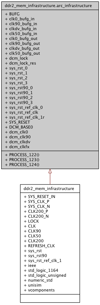
Inheritance diagram for ddr2_mem_infrastructure.arc_infrastructure:
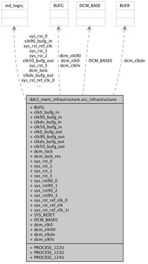
Collaboration diagram for ddr2_mem_infrastructure.arc_infrastructure:
Processes | |
| PROCESS_122 | ( clk0_bufg_out ) |
| shift register for reset | |
| PROCESS_123 | ( clk90_bufg_out ) |
| shift register for reset | |
| PROCESS_124 | ( clk50_bufg_out ) |
| shift register for reset | |
Components | |
| BUFG | |
| global clock buffer | |
Signals | |
| clk0_bufg_in | std_logic |
| clk90_bufg_in | std_logic |
| clkdv_bufg_in | std_logic |
| clk50_bufg_in | std_logic |
| clk0_bufg_out | std_logic |
| clk90_bufg_out | std_logic |
| clkdv_bufg_out | std_logic |
| clk50_bufg_out | std_logic |
| dcm_lock | std_logic |
| dcm_lock_res | std_logic |
| sys_rst_0 | std_logic |
| sys_rst_1 | std_logic |
| sys_rst_2 | std_logic |
| sys_rst_3 | std_logic |
| sys_rst90_0 | std_logic |
| sys_rst90_1 | std_logic |
| sys_rst90_2 | std_logic |
| sys_rst90_3 | std_logic |
| sys_rst_ref_clk_0 | std_logic |
| sys_rst_ref_clk | std_logic |
| sys_rst_ref_clk_1r | std_logic |
| SYS_RESET | std_logic |
Component Instantiations | |
| DCM_BASE0 | DCM_BASE |
| DCM. | |
| dcm_clk0 | BUFG |
| global clock buffer | |
| dcm_clk90 | BUFG |
| global clock buffer | |
| dcm_clkdv | BUFR |
| global clock buffer | |
| dcm_clkfx | BUFG |
| global clock buffer | |
Detailed Description
Services for DDR2 memory controller.This module instantiates the DCM of the FPGA device. The system clock is given as the input and two clocks that are phase shifted by 90 degrees are taken out. It also give the reset signals in phase with the clocks.
Definition at line 84 of file ddr2_mem_infrastructure.vhd.
Member Function Documentation
| PROCESS_122 | ( clk0_bufg_out ) |
shift register for reset
Definition at line 196 of file ddr2_mem_infrastructure.vhd.
00196   process(clk0_bufg_out)
00197   begin
00198     if clk0_bufg_out'event and clk0_bufg_out = '1' then
00199
00200       if ((SYS_RESET = '1') or (dcm_lock = '0') or (sys_rst_ref_clk = '1')) then
00201         sys_rst_0 <= '1';
00202         sys_rst_1 <= '1';
00203         sys_rst_2 <= '1';
00204         sys_rst_3 <= '1';
00205         sys_rst   <= '1';
00206       else
00207         sys_rst_0 <= '0';
00208         sys_rst_1 <= sys_rst_0;
00209         sys_rst_2 <= sys_rst_1;
00210         sys_rst_3 <= sys_rst_2;
00211         sys_rst   <= sys_rst_3;
00212
00213       end if;
00214     end if;
00215   end process;
| PROCESS_123 | ( clk90_bufg_out ) |
shift register for reset
Definition at line 218 of file ddr2_mem_infrastructure.vhd.
00218   process(clk90_bufg_out)
00219   begin
00220     if clk90_bufg_out'event and clk90_bufg_out = '1' then
00221
00222       if ((SYS_RESET = '1') or (dcm_lock = '0') or (sys_rst_ref_clk = '1')) then
00223         sys_rst90_0 <= '1';
00224         sys_rst90_1 <= '1';
00225         sys_rst90_2 <= '1';
00226         sys_rst90_3 <= '1';
00227         sys_rst90   <= '1';
00228       else
00229         sys_rst90_0 <= '0';
00230         sys_rst90_1 <= sys_rst90_0;
00231         sys_rst90_2 <= sys_rst90_1;
00232         sys_rst90_3 <= sys_rst90_2;
00233         sys_rst90   <= sys_rst90_3;
00234       end if;
00235     end if;
00236   end process;
| PROCESS_124 | ( clk50_bufg_out ) |
shift register for reset
Definition at line 239 of file ddr2_mem_infrastructure.vhd.
00239   process(clk50_bufg_out)
00240   begin
00241     if clk50_bufg_out'event and clk50_bufg_out = '1' then
00242
00243       if ((SYS_RESET = '1') or (dcm_lock = '0')) then
00244         sys_rst_ref_clk_0  <= '1';
00245         sys_rst_ref_clk_1r <= '1';
00246         sys_rst_ref_clk    <= '1';
00247       else
00248         sys_rst_ref_clk_0  <= '0';
00249         sys_rst_ref_clk_1r <= sys_rst_ref_clk_0;
00250         sys_rst_ref_clk    <= sys_rst_ref_clk_1r;
00251       end if;
00252     end if;
00253   end process;
Member Data Documentation
BUFG [Component] |
DCM_BASE0 DCM_BASE [Component Instantiation] |
dcm_clkdv BUFR [Component Instantiation] |
The documentation for this class was generated from the following file: