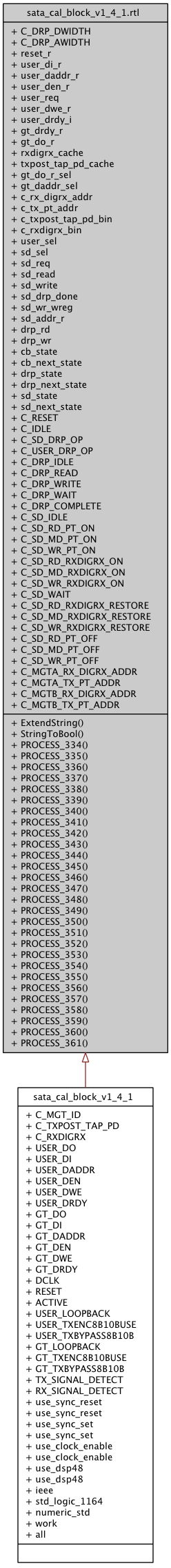
sata_cal_block_v1_4_1.rtl Architecture Reference
calibration logic for SATA RocketIO clocks More...
Functions | |
| string | ExtendString ( string_in: in string , string_len: in integer ) |
| boolean | StringToBool ( S: in string ) |
Processes | |
| PROCESS_334 | ( DCLK , RESET ) |
| Sync RESET. | |
| PROCESS_335 | ( DCLK ) |
| User Data Input. | |
| PROCESS_336 | ( DCLK ) |
| User DRP Address. | |
| PROCESS_337 | ( DCLK ) |
| User Data Write Enable. | |
| PROCESS_338 | ( DCLK ) |
| PROCESS_339 | ( DCLK ) |
| PROCESS_340 | ( DCLK ) |
| User Data Output. | |
| PROCESS_341 | ( DCLK ) |
| User Data Ready. | |
| PROCESS_342 | ( DCLK ) |
| Active signal to indicate a Calibration Block operation. | |
| PROCESS_343 | ( DCLK ) |
| PROCESS_344 | ( DCLK ) |
| PROCESS_345 | ( DCLK ) |
| PROCESS_346 | ( DCLK ) |
| PROCESS_347 | ( DCLK ) |
| PROCESS_348 | ( DCLK ) |
| GT Data Ready. | |
| PROCESS_349 | ( DCLK ) |
| Calibration Block (CB) FSM Reset. | |
| PROCESS_350 | ( cb_state , sd_req , user_req , gt_drdy_r ) |
| Calibration Block (CB) FSM. | |
| PROCESS_351 | ( DCLK ) |
| Signal Detect Request for DRP operation. | |
| PROCESS_352 | ( DCLK ) |
| Indicates Signal Detect DRP Read. | |
| PROCESS_353 | ( DCLK ) |
| Indicates Signal Detect DRP Write. | |
| PROCESS_354 | ( DCLK ) |
| Signal Detect DRP Write Working Register. | |
| PROCESS_355 | ( sd_state ) |
| Generate DRP Addresses for Signal Detect. | |
| PROCESS_356 | ( DCLK ) |
| Assert when Signal Detect DRP Operation is Complete. | |
| PROCESS_357 | ( DCLK ) |
| PROCESS_358 | ( DCLK ) |
| PROCESS_359 | ( sd_state , RX_SIGNAL_DETECT , sd_drp_done ) |
| Signal Detect Block FSM. | |
| PROCESS_360 | ( DCLK ) |
| DRP Read/Write FSM. | |
| PROCESS_361 | ( drp_state , drp_rd , drp_wr , gt_drdy_r ) |
| DRP Read/Write FSM. | |
Constants | |
| C_DRP_DWIDTH | integer := 16 |
| C_DRP_AWIDTH | integer := 8 |
| C_RESET | std_logic_vector ( 3 downto 0 ) := " 0001 " |
| Arbitration FSM. | |
| C_IDLE | std_logic_vector ( 3 downto 0 ) := " 0010 " |
| Arbitration FSM. | |
| C_SD_DRP_OP | std_logic_vector ( 3 downto 0 ) := " 0100 " |
| Arbitration FSM. | |
| C_USER_DRP_OP | std_logic_vector ( 3 downto 0 ) := " 1000 " |
| Arbitration FSM. | |
| C_DRP_IDLE | std_logic_vector ( 4 downto 0 ) := " 00001 " |
| DRP FSM. | |
| C_DRP_READ | std_logic_vector ( 4 downto 0 ) := " 00010 " |
| DRP FSM. | |
| C_DRP_WRITE | std_logic_vector ( 4 downto 0 ) := " 00100 " |
| DRP FSM. | |
| C_DRP_WAIT | std_logic_vector ( 4 downto 0 ) := " 01000 " |
| DRP FSM. | |
| C_DRP_COMPLETE | std_logic_vector ( 4 downto 0 ) := " 10000 " |
| DRP FSM. | |
| C_SD_IDLE | std_logic_vector ( 13 downto 0 ) := " 00000000000001 " |
| Signal Detect Indicator FSM. | |
| C_SD_RD_PT_ON | std_logic_vector ( 13 downto 0 ) := " 00000000000010 " |
| Signal Detect Indicator FSM. | |
| C_SD_MD_PT_ON | std_logic_vector ( 13 downto 0 ) := " 00000000000100 " |
| Signal Detect Indicator FSM. | |
| C_SD_WR_PT_ON | std_logic_vector ( 13 downto 0 ) := " 00000000001000 " |
| Signal Detect Indicator FSM. | |
| C_SD_RD_RXDIGRX_ON | std_logic_vector ( 13 downto 0 ) := " 00000000010000 " |
| Signal Detect Indicator FSM. | |
| C_SD_MD_RXDIGRX_ON | std_logic_vector ( 13 downto 0 ) := " 00000000100000 " |
| Signal Detect Indicator FSM. | |
| C_SD_WR_RXDIGRX_ON | std_logic_vector ( 13 downto 0 ) := " 00000001000000 " |
| Signal Detect Indicator FSM. | |
| C_SD_WAIT | std_logic_vector ( 13 downto 0 ) := " 00000010000000 " |
| Signal Detect Indicator FSM. | |
| C_SD_RD_RXDIGRX_RESTORE | std_logic_vector ( 13 downto 0 ) := " 00000100000000 " |
| Signal Detect Indicator FSM. | |
| C_SD_MD_RXDIGRX_RESTORE | std_logic_vector ( 13 downto 0 ) := " 00001000000000 " |
| Signal Detect Indicator FSM. | |
| C_SD_WR_RXDIGRX_RESTORE | std_logic_vector ( 13 downto 0 ) := " 00010000000000 " |
| Signal Detect Indicator FSM. | |
| C_SD_RD_PT_OFF | std_logic_vector ( 13 downto 0 ) := " 00100000000000 " |
| Signal Detect Indicator FSM. | |
| C_SD_MD_PT_OFF | std_logic_vector ( 13 downto 0 ) := " 01000000000000 " |
| Signal Detect Indicator FSM. | |
| C_SD_WR_PT_OFF | std_logic_vector ( 13 downto 0 ) := " 10000000000000 " |
| Signal Detect Indicator FSM. | |
| C_MGTA_RX_DIGRX_ADDR | std_logic_vector ( 7 downto 0 ) := " 01111101 " |
| Make Addresses for MGTA or MGTB at compile time - 0x7D. | |
| C_MGTA_TX_PT_ADDR | std_logic_vector ( 7 downto 0 ) := " 01001100 " |
| Make Addresses for MGTA or MGTB at compile time - 0x4C. | |
| C_MGTB_RX_DIGRX_ADDR | std_logic_vector ( 7 downto 0 ) := " 01011001 " |
| Make Addresses for MGTA or MGTB at compile time - 0x59. | |
| C_MGTB_TX_PT_ADDR | std_logic_vector ( 7 downto 0 ) := " 01001110 " |
| Make Addresses for MGTA or MGTB at compile time - 0x4E. | |
Signals | |
| reset_r | std_logic_vector ( 1 downto 0 ) |
| user_di_r | std_logic_vector ( C_DRP_DWIDTH-1 downto 0 ) := ( others = > ' 0 ' ) |
| user_daddr_r | std_logic_vector ( C_DRP_AWIDTH-3 downto 0 ) |
| user_den_r | std_logic |
| user_req | std_logic |
| user_dwe_r | std_logic |
| user_drdy_i | std_logic |
| gt_drdy_r | std_logic := ' 0 ' |
| gt_do_r | std_logic_vector ( C_DRP_DWIDTH-1 downto 0 ) := ( others = > ' 0 ' ) |
| rxdigrx_cache | std_logic |
| txpost_tap_pd_cache | std_logic |
| gt_do_r_sel | std_logic_vector ( 2 downto 0 ) |
| gt_daddr_sel | std_logic_vector ( 2 downto 0 ) |
| c_rx_digrx_addr | std_logic_vector ( C_DRP_AWIDTH-1 downto 0 ) |
| c_tx_pt_addr | std_logic_vector ( C_DRP_AWIDTH-1 downto 0 ) |
| c_txpost_tap_pd_bin | std_logic |
| c_rxdigrx_bin | std_logic |
| user_sel | std_logic |
| sd_sel | std_logic |
| sd_req | std_logic := ' 0 ' |
| sd_read | std_logic := ' 0 ' |
| sd_write | std_logic := ' 0 ' |
| sd_drp_done | std_logic := ' 0 ' |
| sd_wr_wreg | std_logic_vector ( C_DRP_DWIDTH-1 downto 0 ) := ( others = > ' 0 ' ) |
| sd_addr_r | std_logic_vector ( C_DRP_AWIDTH-3 downto 0 ) |
| drp_rd | std_logic |
| drp_wr | std_logic |
| cb_state | std_logic_vector ( 3 downto 0 ) |
| cb_next_state | std_logic_vector ( 3 downto 0 ) |
| drp_state | std_logic_vector ( 4 downto 0 ) |
| drp_next_state | std_logic_vector ( 4 downto 0 ) |
| sd_state | std_logic_vector ( 13 downto 0 ) |
| sd_next_state | std_logic_vector ( 13 downto 0 ) |
Detailed Description
calibration logic for SATA RocketIO clocksDefinition at line 136 of file sata_cal_block_v1_4_1.vhd.
Member Function Documentation
| PROCESS_334 | ( DCLK , | |
| RESET ) |
Sync RESET.
Definition at line 313 of file sata_cal_block_v1_4_1.vhd.
00313   process (DCLK, RESET)
00314   begin
00315     if (RESET = '1') then
00316       reset_r <= "11";
00317     elsif (rising_edge(DCLK)) then
00318       reset_r <= '0' & reset_r(1);
00319     end if;
00320   end process;
| PROCESS_335 | ( DCLK ) |
User Data Input.
Definition at line 327 of file sata_cal_block_v1_4_1.vhd.
00327   process (DCLK)
00328   begin
00329     if (rising_edge(DCLK)) then
00330       if (USER_DEN = '1') then
00331         user_di_r <= USER_DI;
00332       end if;
00333     end if;
00334   end process;
| PROCESS_336 | ( DCLK ) |
User DRP Address.
Definition at line 337 of file sata_cal_block_v1_4_1.vhd.
00337   process (DCLK)
00338   begin
00339     if (rising_edge(DCLK)) then
00340       if (USER_DEN = '1') then
00341         user_daddr_r <= USER_DADDR(C_DRP_AWIDTH-3 downto 0);
00342       end if;
00343     end if;
00344   end process;
| PROCESS_337 | ( DCLK ) |
User Data Write Enable.
Definition at line 347 of file sata_cal_block_v1_4_1.vhd.
00347   process (DCLK)
00348   begin
00349     if (rising_edge(DCLK)) then
00350       if (reset_r(0) = '1') then
00351         user_dwe_r <= '0';
00352       elsif (USER_DEN = '1') then
00353         user_dwe_r <= USER_DWE;
00354       end if;
00355     end if;
00356   end process;
| PROCESS_338 | ( DCLK ) |
Register the user_den_r when the user is granted access from the Arbitration FSM
Definition at line 360 of file sata_cal_block_v1_4_1.vhd.
00360   process (DCLK)
00361   begin
00362     if (rising_edge(DCLK)) then
00363       if ((reset_r(0) = '1') or
00364           (cb_state = C_USER_DRP_OP) or
00365           ((USER_DADDR(7) = '1') or (USER_DADDR(6) = '0'))) then
00366         user_den_r <= '0';
00367       elsif (user_den_r = '0') then
00368         user_den_r <= USER_DEN;
00369       end if;
00370     end if;
00371   end process;
| PROCESS_339 | ( DCLK ) |
Generate the user request (user_req) signal when the user is not accessing the same DRP addresses as the Calibration Block or when the Calibration Block is in idle, reset, or wait states.
Definition at line 376 of file sata_cal_block_v1_4_1.vhd.
00376   process (DCLK)
00377   begin
00378     if (rising_edge(DCLK)) then
00379       if ((reset_r(0) = '1') or (cb_state = C_USER_DRP_OP)) then
00380
00381         user_req <= '0';
00382
00383       elsif (
00384         (not(user_daddr_r(5 downto 0) = c_rx_digrx_addr(5 downto 0))) and
00385         (not(user_daddr_r(5 downto 0) = c_tx_pt_addr(5 downto 0)))
00386         ) then
00387
00388         user_req <= user_den_r;
00389
00390       elsif ((sd_state = C_SD_IDLE) or (sd_state = C_SD_WAIT)) then
00391
00392         user_req <= user_den_r;
00393
00394       end if;
00395     end if;
00396   end process;
| PROCESS_340 | ( DCLK ) |
User Data Output.
Definition at line 399 of file sata_cal_block_v1_4_1.vhd.
00399   process (DCLK)
00400   begin
00401     if (rising_edge(DCLK)) then
00402       if ((cb_state = C_USER_DRP_OP) and (GT_DRDY = '1')) then
00403         USER_DO <= GT_DI;
00404       end if;
00405     end if;
00406   end process;
| PROCESS_341 | ( DCLK ) |
User Data Ready.
Definition at line 409 of file sata_cal_block_v1_4_1.vhd.
00409   process (DCLK)
00410   begin
00411     if (rising_edge(DCLK)) then
00412       if ((reset_r(0) = '1') or (user_drdy_i = '1')) then
00413         user_drdy_i <= '0';
00414       elsif (cb_state = C_USER_DRP_OP) then
00415         user_drdy_i <= GT_DRDY;
00416       end if;
00417     end if;
00418   end process;
| PROCESS_342 | ( DCLK ) |
Active signal to indicate a Calibration Block operation.
Definition at line 423 of file sata_cal_block_v1_4_1.vhd.
00423   process (DCLK)
00424   begin
00425     if (rising_edge(DCLK)) then
00426       if (cb_state = C_RESET) then
00427         ACTIVE <= '0';
00428       else
00429         if ((not (cb_state = C_IDLE)) and
00430             (not (cb_state = C_USER_DRP_OP))) then
00431           ACTIVE <= '1';
00432         else
00433           ACTIVE <= '0';
00434         end if;
00435       end if;
00436     end if;
00437   end process;
| PROCESS_343 | ( DCLK ) |
Storing the value of RXDIGRX. The value is written from the default parameter upon reset or when the user writes to DRP register in those bits location.
Definition at line 442 of file sata_cal_block_v1_4_1.vhd.
00442   process (DCLK)
00443   begin
00444     if (rising_edge(DCLK)) then
00445       if (reset_r(0) = '1') then
00446         rxdigrx_cache <= c_rxdigrx_bin;
00447       elsif ((drp_state = C_DRP_WRITE) and
00448              (cb_state = C_USER_DRP_OP) and
00449              (user_daddr_r(5 downto 0) = c_rx_digrx_addr(5 downto 0))) then
00450         rxdigrx_cache <= user_di_r(1);
00451       end if;
00452     end if;
00453   end process;
| PROCESS_344 | ( DCLK ) |
Storing the value of TXPOST_TAP_PD. The value is written from the default parameter upon reset or when the user writes to DRP register in those bits location.
Definition at line 458 of file sata_cal_block_v1_4_1.vhd.
00458   process (DCLK)
00459   begin
00460     if (rising_edge(DCLK)) then
00461       if (reset_r(0) = '1') then
00462         txpost_tap_pd_cache <= c_txpost_tap_pd_bin;
00463       elsif ((drp_state = C_DRP_WRITE) and
00464              (cb_state = C_USER_DRP_OP) and
00465              (user_daddr_r(5 downto 0) = c_tx_pt_addr(5 downto 0))) then
00466         txpost_tap_pd_cache <= user_di_r(12);
00467       end if;
00468     end if;
00469   end process;
| PROCESS_345 | ( DCLK ) |
GT Data Output: the data output is generated either from a Signal Detect FSM operation or a user access.
Definition at line 479 of file sata_cal_block_v1_4_1.vhd.
00479   process (DCLK)
00480   begin
00481     if (rising_edge(DCLK)) then
00482
00483       if (gt_do_r_sel(2) = '1') then
00484         gt_do_r <= sd_wr_wreg;
00485       elsif (gt_do_r_sel = "001") then
00486         gt_do_r <= user_di_r;
00487       else
00488         null;
00489       end if;
00490
00491     end if;
00492   end process;
| PROCESS_346 | ( DCLK ) |
GT DRP Address: the DRP address is generated either from a Signal Detect FSM operation, or a user access. DRP address ranges from 0x40 to 0x7F.
Definition at line 500 of file sata_cal_block_v1_4_1.vhd.
00500   process (DCLK)
00501   begin
00502     if (rising_edge(DCLK)) then
00503
00504       if (gt_daddr_sel(2) = '1') then
00505         GT_DADDR(5 downto 0) <= sd_addr_r(5 downto 0);
00506       elsif (gt_daddr_sel = "001") then
00507         GT_DADDR(5 downto 0) <= user_daddr_r(5 downto 0);
00508       else
00509         null;
00510       end if;
00511
00512       GT_DADDR(7 downto 6) <= "01";
00513
00514     end if;
00515   end process;
| PROCESS_347 | ( DCLK ) |
GT Data Enable: the data enable is generated whenever there is a DRP Read or a DRP Write
Definition at line 519 of file sata_cal_block_v1_4_1.vhd.
00519   process (DCLK)
00520   begin
00521     if (rising_edge(DCLK)) then
00522       if (reset_r(0) = '1') then
00523         GT_DEN <= '0';
00524       else
00525         if ((drp_state = C_DRP_IDLE) and
00526             ((drp_wr = '1') or (drp_rd = '1'))) then
00527           GT_DEN <= '1';
00528         else
00529           GT_DEN <= '0';
00530         end if;
00531       end if;
00532     end if;
00533   end process;
| PROCESS_348 | ( DCLK ) |
GT Data Ready.
Definition at line 539 of file sata_cal_block_v1_4_1.vhd.
00539   process (DCLK)
00540   begin
00541     if (rising_edge(DCLK)) then
00542       gt_drdy_r <= GT_DRDY;
00543     end if;
00544   end process;
| PROCESS_349 | ( DCLK ) |
Calibration Block (CB) FSM Reset.
Definition at line 558 of file sata_cal_block_v1_4_1.vhd.
00558   process (DCLK)
00559   begin
00560     if (rising_edge(DCLK)) then
00561       if (reset_r(0) = '1') then
00562         cb_state <= C_RESET;
00563       else
00564         cb_state <= cb_next_state;
00565       end if;
00566     end if;
00567   end process;
| PROCESS_350 | ( cb_state , | |
| sd_req , | ||
| user_req , | ||
| gt_drdy_r ) |
Calibration Block (CB) FSM.
Definition at line 570 of file sata_cal_block_v1_4_1.vhd.
00570   process (cb_state, sd_req, user_req, gt_drdy_r)
00571     variable cb_fsm_name : string(1 to 25);
00572   begin
00573     case cb_state is
00574
00575       when C_RESET =>
00576
00577         cb_next_state <= C_IDLE;
00578         cb_fsm_name   := ExtendString("C_RESET", 25);
00579
00580       when C_IDLE =>
00581
00582         if (sd_req = '1') then
00583           cb_next_state <= C_SD_DRP_OP;
00584         elsif (user_req = '1') then
00585           cb_next_state <= C_USER_DRP_OP;
00586         else
00587           cb_next_state <= C_IDLE;
00588         end if;
00589
00590         cb_fsm_name := ExtendString("C_IDLE", 25);
00591
00592       when C_SD_DRP_OP =>
00593
00594         if (gt_drdy_r = '1') then
00595           cb_next_state <= C_IDLE;
00596         else
00597           cb_next_state <= C_SD_DRP_OP;
00598         end if;
00599
00600         cb_fsm_name := ExtendString("C_SD_DRP_OP", 25);
00601
00602       when C_USER_DRP_OP =>
00603
00604         if (gt_drdy_r = '1') then
00605           cb_next_state <= C_IDLE;
00606         else
00607           cb_next_state <= C_USER_DRP_OP;
00608         end if;
00609
00610         cb_fsm_name := ExtendString("C_USER_DRP_OP", 25);
00611
00612       when others =>
00613
00614         cb_next_state <= C_IDLE;
00615         cb_fsm_name   := ExtendString("default", 25);
00616
00617     end case;
00618   end process;
| PROCESS_351 | ( DCLK ) |
Signal Detect Request for DRP operation.
Definition at line 624 of file sata_cal_block_v1_4_1.vhd.
00624   process (DCLK)
00625   begin
00626     if (rising_edge(DCLK)) then
00627       if ((sd_state = C_SD_IDLE) or (sd_drp_done = '1')) then
00628         sd_req <= '0';
00629       else
00630         sd_req <= sd_read or sd_write;
00631       end if;
00632     end if;
00633   end process;
| PROCESS_352 | ( DCLK ) |
Indicates Signal Detect DRP Read.
Definition at line 636 of file sata_cal_block_v1_4_1.vhd.
00636   process (DCLK)
00637   begin
00638     if (rising_edge(DCLK)) then
00639       if ((sd_state = C_SD_IDLE) or (sd_drp_done = '1')) then
00640         sd_read <= '0';
00641       else
00642         if ((sd_state = C_SD_RD_PT_ON) or
00643             (sd_state = C_SD_RD_RXDIGRX_ON) or
00644             (sd_state = C_SD_RD_RXDIGRX_RESTORE) or
00645             (sd_state = C_SD_RD_PT_OFF)) then
00646           sd_read <= '1';
00647         else
00648           sd_read <= '0';
00649         end if;
00650       end if;
00651     end if;
00652   end process;
| PROCESS_353 | ( DCLK ) |
Indicates Signal Detect DRP Write.
Definition at line 655 of file sata_cal_block_v1_4_1.vhd.
00655   process (DCLK)
00656   begin
00657     if (rising_edge(DCLK)) then
00658       if ((sd_state = C_SD_IDLE) or (sd_drp_done = '1')) then
00659         sd_write <= '0';
00660       else
00661         if ((sd_state = C_SD_WR_PT_ON) or
00662             (sd_state = C_SD_WR_RXDIGRX_ON) or
00663             (sd_state = C_SD_WR_RXDIGRX_RESTORE) or
00664             (sd_state = C_SD_WR_PT_OFF)) then
00665           sd_write <= '1';
00666         else
00667           sd_write <= '0';
00668         end if;
00669       end if;
00670     end if;
00671   end process;
| PROCESS_354 | ( DCLK ) |
Signal Detect DRP Write Working Register.
Definition at line 674 of file sata_cal_block_v1_4_1.vhd.
00674   process (DCLK)
00675   begin
00676     if (rising_edge(DCLK)) then
00677       if ((cb_state = C_SD_DRP_OP) and (sd_read = '1') and (GT_DRDY = '1')) then
00678         sd_wr_wreg <= GT_DI;
00679       else
00680         case sd_state is
00681
00682           when C_SD_MD_PT_ON =>
00683             sd_wr_wreg <= sd_wr_wreg(15 downto 13) & '0' &
00684                           sd_wr_wreg(11 downto 0);
00685           when C_SD_MD_RXDIGRX_ON =>
00686             sd_wr_wreg <= sd_wr_wreg(15 downto 2) & '1' & sd_wr_wreg(0);
00687           when C_SD_MD_RXDIGRX_RESTORE =>
00688             sd_wr_wreg <= sd_wr_wreg(15 downto 2) & rxdigrx_cache &
00689                           sd_wr_wreg(0);
00690           when C_SD_MD_PT_OFF =>
00691             sd_wr_wreg <= sd_wr_wreg(15 downto 13) & txpost_tap_pd_cache &
00692                           sd_wr_wreg(11 downto 0);
00693           when others =>
00694             null;
00695         end case;
00696       end if;
00697     end if;
00698   end process;
| PROCESS_355 | ( sd_state ) |
Generate DRP Addresses for Signal Detect.
Definition at line 701 of file sata_cal_block_v1_4_1.vhd.
00701   process (sd_state)
00702   begin
00703     case sd_state is
00704       when C_SD_RD_PT_ON =>
00705         sd_addr_r(5 downto 0) <= c_tx_pt_addr(5 downto 0);
00706       when C_SD_WR_PT_ON =>
00707         sd_addr_r(5 downto 0) <= c_tx_pt_addr(5 downto 0);
00708       when C_SD_RD_PT_OFF =>
00709         sd_addr_r(5 downto 0) <= c_tx_pt_addr(5 downto 0);
00710       when C_SD_WR_PT_OFF =>
00711         sd_addr_r(5 downto 0) <= c_tx_pt_addr(5 downto 0);
00712       when C_SD_RD_RXDIGRX_ON =>
00713         sd_addr_r(5 downto 0) <= c_rx_digrx_addr(5 downto 0);
00714       when C_SD_WR_RXDIGRX_ON =>
00715         sd_addr_r(5 downto 0) <= c_rx_digrx_addr(5 downto 0);
00716       when C_SD_RD_RXDIGRX_RESTORE =>
00717         sd_addr_r(5 downto 0) <= c_rx_digrx_addr(5 downto 0);
00718       when C_SD_WR_RXDIGRX_RESTORE =>
00719         sd_addr_r(5 downto 0) <= c_rx_digrx_addr(5 downto 0);
00720       when others =>
00721         sd_addr_r(5 downto 0) <= c_tx_pt_addr(5 downto 0);
00722     end case;
00723   end process;
| PROCESS_356 | ( DCLK ) |
Assert when Signal Detect DRP Operation is Complete.
Definition at line 726 of file sata_cal_block_v1_4_1.vhd.
00726   process (DCLK)
00727   begin
00728     if (rising_edge(DCLK)) then
00729       if ((GT_DRDY = '1') and (cb_state = C_SD_DRP_OP)) then
00730         sd_drp_done <= '1';
00731       else
00732         sd_drp_done <= '0';
00733       end if;
00734     end if;
00735   end process;
| PROCESS_357 | ( DCLK ) |
GT_LOOPBACK, GT_TXENC8B10BUSE and GT_TXBYPASS8B10B Switch the GT11 to serial loopback mode and enable 8B10B when the Signal Detect is Low.
Definition at line 740 of file sata_cal_block_v1_4_1.vhd.
00740   process (DCLK)
00741   begin
00742     if (rising_edge(DCLK)) then
00743       if (reset_r(0) = '1') then
00744         GT_LOOPBACK <= "00";
00745       elsif (RX_SIGNAL_DETECT = '0') then
00746         GT_LOOPBACK <= "11";
00747       else
00748         GT_LOOPBACK <= USER_LOOPBACK;
00749       end if;
00750     end if;
00751   end process;
| PROCESS_358 | ( DCLK ) |
Signal Detect Block FSM: The SD FSM is triggered when RX_SIGNAL_DETECT goes Low
Definition at line 762 of file sata_cal_block_v1_4_1.vhd.
00762   process (DCLK)
00763   begin
00764     if (rising_edge(DCLK)) then
00765       if (reset_r(0) = '1') then
00766         sd_state <= C_SD_IDLE;
00767       else
00768         sd_state <= sd_next_state;
00769       end if;
00770     end if;
00771   end process;
| PROCESS_359 | ( sd_state , | |
| RX_SIGNAL_DETECT , | ||
| sd_drp_done ) |
Signal Detect Block FSM.
Definition at line 774 of file sata_cal_block_v1_4_1.vhd.
00774   process (sd_state, RX_SIGNAL_DETECT, sd_drp_done)
00775     variable sd_fsm_name : string(1 to 25);
00776   begin
00777     case sd_state is
00778
00779       when C_SD_IDLE =>
00780
00781         if (RX_SIGNAL_DETECT = '0') then
00782           sd_next_state <= C_SD_RD_PT_ON;
00783         else
00784           sd_next_state <= C_SD_IDLE;
00785         end if;
00786
00787         sd_fsm_name := ExtendString("C_SD_IDLE", 25);
00788
00789       when C_SD_RD_PT_ON =>
00790
00791         if (sd_drp_done = '1') then
00792           sd_next_state <= C_SD_MD_PT_ON;
00793         else
00794           sd_next_state <= C_SD_RD_PT_ON;
00795         end if;
00796
00797         sd_fsm_name := ExtendString("C_SD_RD_PT_ON", 25);
00798
00799       when C_SD_MD_PT_ON =>
00800
00801         sd_next_state <= C_SD_WR_PT_ON;
00802         sd_fsm_name   := ExtendString("C_SD_MD_PT_ON", 25);
00803
00804       when C_SD_WR_PT_ON =>
00805
00806         if (sd_drp_done = '1') then
00807           sd_next_state <= C_SD_RD_RXDIGRX_ON;
00808         else
00809           sd_next_state <= C_SD_WR_PT_ON;
00810         end if;
00811
00812         sd_fsm_name := ExtendString("C_SD_WR_PT_ON", 25);
00813
00814       when C_SD_RD_RXDIGRX_ON =>
00815
00816         if (sd_drp_done = '1') then
00817           sd_next_state <= C_SD_MD_RXDIGRX_ON;
00818         else
00819           sd_next_state <= C_SD_RD_RXDIGRX_ON;
00820         end if;
00821
00822         sd_fsm_name := ExtendString("C_SD_RD_RXDIGRX_ON", 25);
00823
00824       when C_SD_MD_RXDIGRX_ON =>
00825
00826         sd_next_state <= C_SD_WR_RXDIGRX_ON;
00827         sd_fsm_name   := ExtendString("C_SD_MD_RXDIGRX_ON", 25);
00828
00829       when C_SD_WR_RXDIGRX_ON =>
00830
00831         if (sd_drp_done = '1') then
00832           sd_next_state <= C_SD_WAIT;
00833         else
00834           sd_next_state <= C_SD_WR_RXDIGRX_ON;
00835         end if;
00836
00837         sd_fsm_name := ExtendString("C_SD_WR_RXDIGRX_ON", 25);
00838
00839       when C_SD_WAIT =>
00840
00841         if (RX_SIGNAL_DETECT = '1') then
00842           sd_next_state <= C_SD_RD_RXDIGRX_RESTORE;
00843         else
00844           sd_next_state <= C_SD_WAIT;
00845         end if;
00846
00847         sd_fsm_name := ExtendString("C_SD_WAIT", 25);
00848
00849       when C_SD_RD_RXDIGRX_RESTORE =>
00850
00851         if (sd_drp_done = '1') then
00852           sd_next_state <= C_SD_MD_RXDIGRX_RESTORE;
00853         else
00854           sd_next_state <= C_SD_RD_RXDIGRX_RESTORE;
00855         end if;
00856
00857         sd_fsm_name := ExtendString("C_SD_RD_RXDIGRX_RESTORE", 25);
00858
00859       when C_SD_MD_RXDIGRX_RESTORE =>
00860
00861         sd_next_state <= C_SD_WR_RXDIGRX_RESTORE;
00862         sd_fsm_name   := ExtendString("C_SD_MD_RXDIGRX_RESTORE", 25);
00863
00864       when C_SD_WR_RXDIGRX_RESTORE =>
00865
00866         if (sd_drp_done = '1') then
00867           sd_next_state <= C_SD_RD_PT_OFF;
00868         else
00869           sd_next_state <= C_SD_WR_RXDIGRX_RESTORE;
00870         end if;
00871
00872         sd_fsm_name := ExtendString("C_SD_WR_RXDIGRX_RESTORE", 25);
00873
00874       when C_SD_RD_PT_OFF =>
00875
00876         if (sd_drp_done = '1') then
00877           sd_next_state <= C_SD_MD_PT_OFF;
00878         else
00879           sd_next_state <= C_SD_RD_PT_OFF;
00880         end if;
00881
00882         sd_fsm_name := ExtendString("C_SD_RD_PT_OFF", 25);
00883
00884       when C_SD_MD_PT_OFF =>
00885
00886         sd_next_state <= C_SD_WR_PT_OFF;
00887         sd_fsm_name   := ExtendString("C_SD_MD_PT_OFF", 25);
00888
00889       when C_SD_WR_PT_OFF =>
00890
00891         if (sd_drp_done = '1') then
00892           sd_next_state <= C_SD_IDLE;
00893         else
00894           sd_next_state <= C_SD_WR_PT_OFF;
00895         end if;
00896
00897         sd_fsm_name := ExtendString("C_SD_WR_PT_OFF", 25);
00898
00899       when others =>
00900
00901         sd_next_state <= C_SD_IDLE;
00902         sd_fsm_name   := ExtendString("default", 25);
00903
00904     end case;
00905   end process;
| PROCESS_360 | ( DCLK ) |
DRP Read/Write FSM.
Definition at line 922 of file sata_cal_block_v1_4_1.vhd.
00922   process (DCLK)
00923   begin
00924     if (rising_edge(DCLK)) then
00925       if (reset_r(0) = '1') then
00926         drp_state <= C_DRP_IDLE;
00927       else
00928         drp_state <= drp_next_state;
00929       end if;
00930     end if;
00931   end process;
| PROCESS_361 | ( drp_state , | |
| drp_rd , | ||
| drp_wr , | ||
| gt_drdy_r ) |
DRP Read/Write FSM.
Definition at line 934 of file sata_cal_block_v1_4_1.vhd.
00934   process (drp_state, drp_rd, drp_wr, gt_drdy_r)
00935     variable drp_fsm_name : string(1 to 25);
00936   begin
00937     case drp_state is
00938       when C_DRP_IDLE =>
00939
00940         if (drp_wr = '1') then
00941           drp_next_state <= C_DRP_WRITE;
00942         else
00943           if (drp_rd = '1') then
00944             drp_next_state <= C_DRP_READ;
00945           else
00946             drp_next_state <= C_DRP_IDLE;
00947           end if;
00948         end if;
00949
00950         drp_fsm_name := ExtendString("C_DRP_IDLE", 25);
00951
00952       when C_DRP_READ =>
00953
00954         drp_next_state <= C_DRP_WAIT;
00955         drp_fsm_name   := ExtendString("C_DRP_READ", 25);
00956
00957       when C_DRP_WRITE =>
00958
00959         drp_next_state <= C_DRP_WAIT;
00960         drp_fsm_name   := ExtendString("C_DRP_WRITE", 25);
00961
00962       when C_DRP_WAIT =>
00963
00964         if (gt_drdy_r = '1') then
00965           drp_next_state <= C_DRP_COMPLETE;
00966         else
00967           drp_next_state <= C_DRP_WAIT;
00968         end if;
00969
00970         drp_fsm_name := ExtendString("C_DRP_WAIT", 25);
00971
00972       when C_DRP_COMPLETE =>
00973
00974         drp_next_state <= C_DRP_IDLE;
00975         drp_fsm_name   := ExtendString("C_DRP_COMPLETE", 25);
00976
00977       when others =>
00978         drp_next_state <= C_DRP_IDLE;
00979         drp_fsm_name   := ExtendString("default", 25);
00980
00981     end case;
00982   end process;
Member Data Documentation
C_DRP_COMPLETE std_logic_vector ( 4 downto 0 ) := " 10000 " [Constant] |
C_DRP_IDLE std_logic_vector ( 4 downto 0 ) := " 00001 " [Constant] |
C_DRP_READ std_logic_vector ( 4 downto 0 ) := " 00010 " [Constant] |
C_DRP_WAIT std_logic_vector ( 4 downto 0 ) := " 01000 " [Constant] |
C_DRP_WRITE std_logic_vector ( 4 downto 0 ) := " 00100 " [Constant] |
C_IDLE std_logic_vector ( 3 downto 0 ) := " 0010 " [Constant] |
C_MGTA_RX_DIGRX_ADDR std_logic_vector ( 7 downto 0 ) := " 01111101 " [Constant] |
Make Addresses for MGTA or MGTB at compile time - 0x7D.
Definition at line 260 of file sata_cal_block_v1_4_1.vhd.
C_MGTA_TX_PT_ADDR std_logic_vector ( 7 downto 0 ) := " 01001100 " [Constant] |
Make Addresses for MGTA or MGTB at compile time - 0x4C.
Definition at line 262 of file sata_cal_block_v1_4_1.vhd.
C_MGTB_RX_DIGRX_ADDR std_logic_vector ( 7 downto 0 ) := " 01011001 " [Constant] |
Make Addresses for MGTA or MGTB at compile time - 0x59.
Definition at line 264 of file sata_cal_block_v1_4_1.vhd.
C_MGTB_TX_PT_ADDR std_logic_vector ( 7 downto 0 ) := " 01001110 " [Constant] |
Make Addresses for MGTA or MGTB at compile time - 0x4E.
Definition at line 266 of file sata_cal_block_v1_4_1.vhd.
C_RESET std_logic_vector ( 3 downto 0 ) := " 0001 " [Constant] |
C_SD_DRP_OP std_logic_vector ( 3 downto 0 ) := " 0100 " [Constant] |
C_SD_IDLE std_logic_vector ( 13 downto 0 ) := " 00000000000001 " [Constant] |
C_SD_MD_PT_OFF std_logic_vector ( 13 downto 0 ) := " 01000000000000 " [Constant] |
C_SD_MD_PT_ON std_logic_vector ( 13 downto 0 ) := " 00000000000100 " [Constant] |
C_SD_MD_RXDIGRX_ON std_logic_vector ( 13 downto 0 ) := " 00000000100000 " [Constant] |
C_SD_MD_RXDIGRX_RESTORE std_logic_vector ( 13 downto 0 ) := " 00001000000000 " [Constant] |
C_SD_RD_PT_OFF std_logic_vector ( 13 downto 0 ) := " 00100000000000 " [Constant] |
C_SD_RD_PT_ON std_logic_vector ( 13 downto 0 ) := " 00000000000010 " [Constant] |
C_SD_RD_RXDIGRX_ON std_logic_vector ( 13 downto 0 ) := " 00000000010000 " [Constant] |
C_SD_RD_RXDIGRX_RESTORE std_logic_vector ( 13 downto 0 ) := " 00000100000000 " [Constant] |
C_SD_WAIT std_logic_vector ( 13 downto 0 ) := " 00000010000000 " [Constant] |
C_SD_WR_PT_OFF std_logic_vector ( 13 downto 0 ) := " 10000000000000 " [Constant] |
C_SD_WR_PT_ON std_logic_vector ( 13 downto 0 ) := " 00000000001000 " [Constant] |
C_SD_WR_RXDIGRX_ON std_logic_vector ( 13 downto 0 ) := " 00000001000000 " [Constant] |
C_SD_WR_RXDIGRX_RESTORE std_logic_vector ( 13 downto 0 ) := " 00010000000000 " [Constant] |
C_USER_DRP_OP std_logic_vector ( 3 downto 0 ) := " 1000 " [Constant] |
The documentation for this class was generated from the following file: