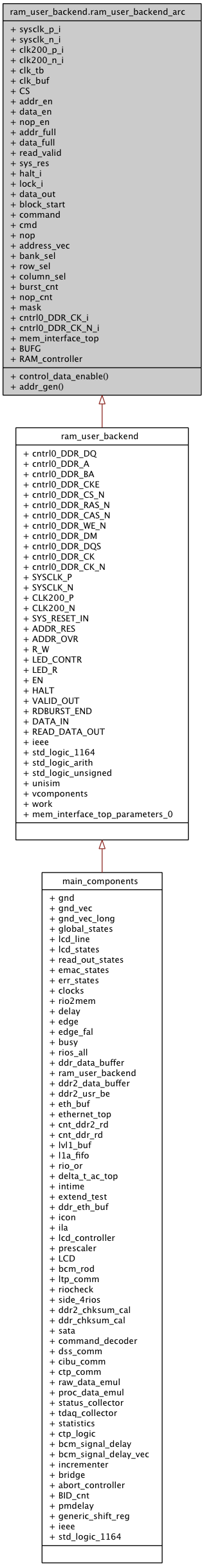
ram_user_backend.ram_user_backend_arc Architecture Reference
Control of interface to external RAM. More...
Inheritance diagram for ram_user_backend.ram_user_backend_arc:
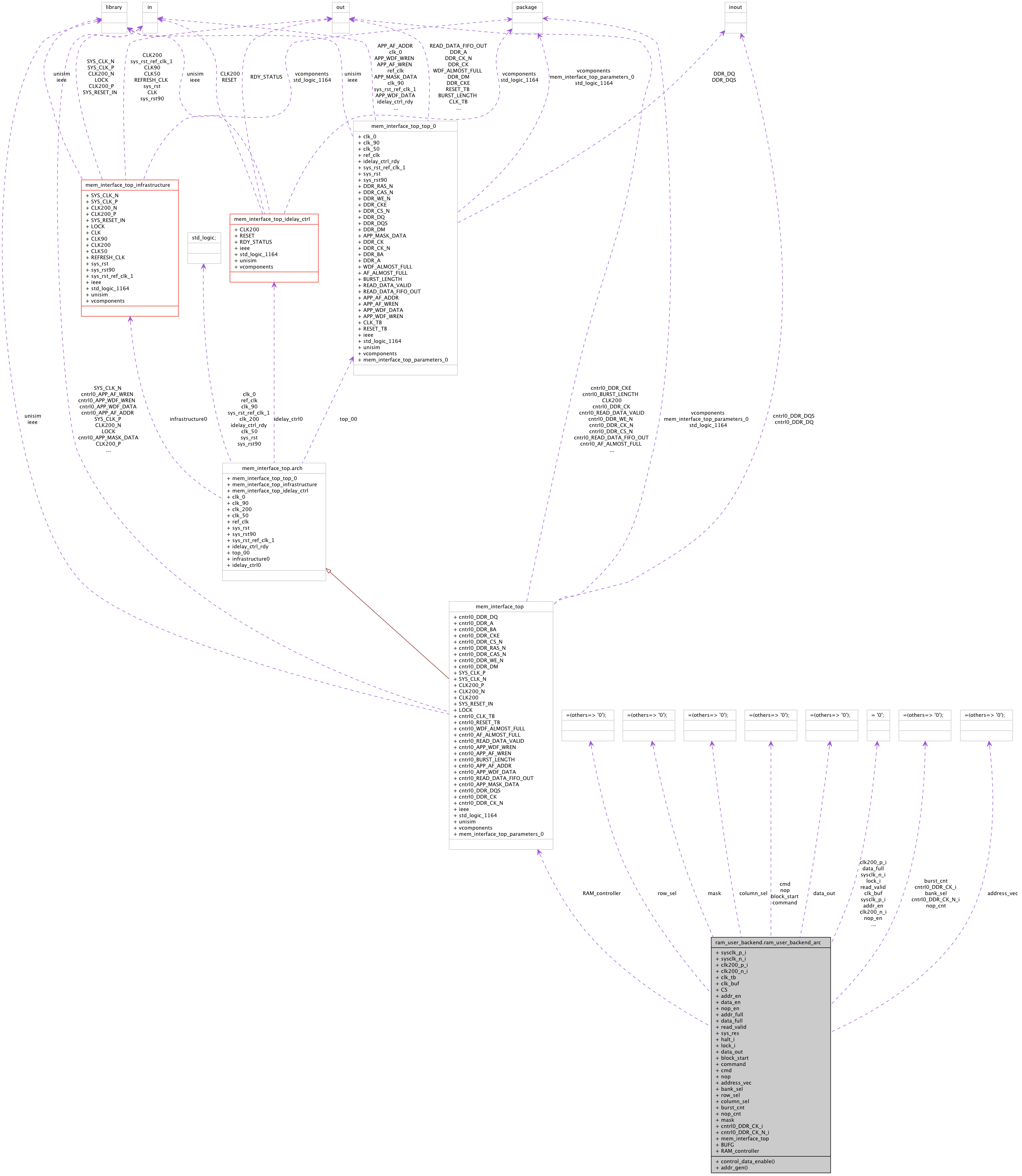
Collaboration diagram for ram_user_backend.ram_user_backend_arc:
Processes | |
| control_data_enable | ( clk_buf ) |
| control write enable | |
| addr_gen | ( clk_buf ) |
| address generation | |
Components | |
| mem_interface_top | <Entity mem_interface_top> |
| RAM controller. | |
| BUFG | |
| global clock buffer | |
Signals | |
| sysclk_p_i | std_logic := ' 0 ' |
| sysclk_n_i | std_logic := ' 0 ' |
| clk200_p_i | std_logic := ' 0 ' |
| clk200_n_i | std_logic := ' 0 ' |
| clk_tb | std_logic := ' 0 ' |
| clk_buf | std_logic := ' 0 ' |
| CS | std_logic := ' 0 ' |
| addr_en | std_logic := ' 0 ' |
| data_en | std_logic := ' 0 ' |
| nop_en | std_logic := ' 0 ' |
| addr_full | std_logic := ' 0 ' |
| data_full | std_logic := ' 0 ' |
| read_valid | std_logic := ' 0 ' |
| sys_res | std_logic := ' 0 ' |
| halt_i | std_logic := ' 0 ' |
| lock_i | std_logic := ' 0 ' |
| data_out | std_logic_vector ( 63 downto 0 ) := ( others = > ' 0 ' ) |
| block_start | std_logic_vector ( 2 downto 0 ) := ( others = > ' 0 ' ) |
| command | std_logic_vector ( 2 downto 0 ) := ( others = > ' 0 ' ) |
| cmd | std_logic_vector ( 2 downto 0 ) := ( others = > ' 0 ' ) |
| nop | std_logic_vector ( 2 downto 0 ) := ( others = > ' 0 ' ) |
| address_vec | std_logic_vector ( 35 downto 0 ) := ( others = > ' 0 ' ) |
| bank_sel | std_logic_vector ( 1 downto 0 ) := ( others = > ' 0 ' ) |
| row_sel | std_logic_vector ( 12 downto 0 ) := ( others = > ' 0 ' ) |
| column_sel | std_logic_vector ( 5 downto 0 ) := ( others = > ' 0 ' ) |
| burst_cnt | std_logic_vector ( 1 downto 0 ) := ( others = > ' 0 ' ) |
| nop_cnt | std_logic_vector ( 1 downto 0 ) := ( others = > ' 0 ' ) |
| mask | std_logic_vector ( 7 downto 0 ) := ( others = > ' 0 ' ) |
| cntrl0_DDR_CK_i | std_logic_vector ( 1 downto 0 ) := ( others = > ' 0 ' ) |
| cntrl0_DDR_CK_N_i | std_logic_vector ( 1 downto 0 ) := ( others = > ' 0 ' ) |
Component Instantiations | |
| RAM_controller | mem_interface_top <Entity mem_interface_top> |
Detailed Description
Control of interface to external RAM.Contains an FSM plus support logic for controlling the external RAM. It generates the addresses in a cyclic fashion and takes care of the correct burst timing structure. Also contains a couple of waits to avoid to high pressure in the data path during continuos capturing.
Definition at line 82 of file ram_user_backend.vhd.
Member Function Documentation
| addr_gen | ( clk_buf ) |
address generation
FSM generates addresses (row, column) in cyclic way and takes care of correct burst timing structure. Different modes and timing for read and write. More pauses during read.
Definition at line 213 of file ram_user_backend.vhd.
00213   addr_gen : process(clk_buf)
00214   begin
00215     if clk_buf'event and clk_buf = '1' then
00216
00217       if (sys_res or ADDR_RES) = '1' then
00218         column_sel <= (others => '0');
00219         bank_sel   <= (others => '0');
00220         row_sel    <= (others => '0');
00221         burst_cnt  <= "00";
00222         nop_cnt    <= "00";
00223         addr_en    <= '0';
00224         nop_en     <= '0';
00225
00226       elsif addr_full = '0' and EN = '1' then  --stop_write = '0' then
00227
00228         burst_cnt <= burst_cnt + 1;
00229
00230         if R_W = '0' and data_full = '0' then
00231
00232           if burst_cnt = "11" then
00233             if nop_en = '1' then
00234               addr_en <= '0';
00235             else
00236               addr_en <= '1';
00237             end if;
00238             nop_cnt <= nop_cnt + 1;
00239           else
00240             addr_en <= '0';
00241             nop_cnt <= nop_cnt;
00242           end if;
00243
00244           if burst_cnt = "10" then
00245             if nop_cnt = "11" then
00246               nop_en     <= '1';
00247               bank_sel   <= bank_sel;
00248               column_sel <= column_sel;
00249               row_sel    <= row_sel;
00250             else
00251               nop_en <= '0';
00252             end if;
00253           end if;
00254
00255           if nop_en = '0' then
00256             if burst_cnt = "11" then
00257               column_sel <= column_sel + 1;
00258               if column_sel = "111111" then
00259                 bank_sel   <= bank_sel + 1;
00260                 column_sel <= (others => '0');
00261                 if bank_sel = "11" then
00262                   row_sel  <= row_sel + 1;
00263                   bank_sel <= "00";
00264
00265                 else
00266                   row_sel <= row_sel;
00267                 end if;
00268               else
00269                 bank_sel <= bank_sel;
00270               end if;
00271             else
00272               column_sel <= column_sel;
00273             end if;
00274           end if;
00275
00276         else
00277
00278           if burst_cnt = "11" then
00279             if nop_en = '1' then
00280               addr_en <= '0';
00281             else
00282               addr_en <= '1';
00283             end if;
00284             nop_en <= not nop_en;
00285           else
00286             addr_en <= '0';
00287             nop_cnt <= nop_cnt;
00288           end if;
00289
00290           if nop_en = '0' then
00291             if burst_cnt = "11" then
00292               column_sel <= column_sel + 1;
00293               if column_sel = "111111" then
00294                 bank_sel   <= bank_sel + 1;
00295                 column_sel <= (others => '0');
00296                 if bank_sel = "11" then
00297                   row_sel  <= row_sel + 1;
00298                   bank_sel <= "00";
00299                 else
00300                   row_sel <= row_sel;
00301                 end if;
00302               else
00303                 bank_sel <= bank_sel;
00304               end if;
00305             else
00306               column_sel <= column_sel;
00307             end if;
00308           end if;
00309
00310         end if;
00311
00312       elsif R_W = '0' and EN = '0' then
00313         addr_en <= '0';
00314         nop_en  <= '0';
00315         nop_cnt <= (others => '0');
00316
00317       else
00318
00319         addr_en <= '0';
00320
00321       end if;
00322     end if;
00323   end process addr_gen;
| control_data_enable | ( clk_buf ) |
control write enable
Definition at line 198 of file ram_user_backend.vhd.
00198   control_data_enable : process(clk_buf)
00199   begin
00200     if clk_buf'event and clk_buf = '1' then
00201       if R_W = '0' and data_full = '0' and nop_en = '0' then
00202         data_en <= '1';
00203       else
00204         data_en <= '0';
00205       end if;
00206     end if;
00207   end process control_data_enable;
Member Data Documentation
BUFG [Component] |
mem_interface_top [Component] |
RAM_controller mem_interface_top [Component Instantiation] |
RAM controller instance
Definition at line 326 of file ram_user_backend.vhd.
The documentation for this class was generated from the following file: