mem_interface_top_infrastructure.arch Architecture Reference
DCM for DDR specific clocks. More...
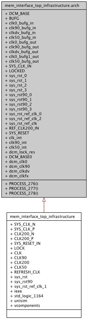
Inheritance diagram for mem_interface_top_infrastructure.arch:
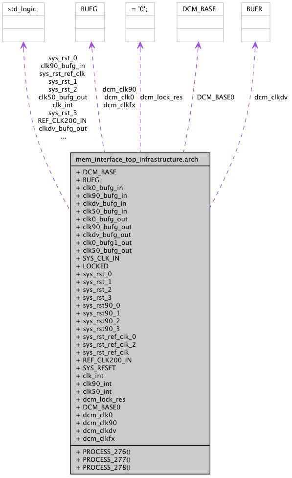
Collaboration diagram for mem_interface_top_infrastructure.arch:
Processes | |
| PROCESS_276 | ( clk_int ) |
| PROCESS_277 | ( clk90_int ) |
| PROCESS_278 | ( clk50_int ) |
Components | |
| DCM_BASE | |
| Virtex-4 DCM. | |
| BUFG | |
| global clock buffer | |
Signals | |
| clk0_bufg_in | std_logic |
| clk90_bufg_in | std_logic |
| clkdv_bufg_in | std_logic |
| clk50_bufg_in | std_logic |
| clk0_bufg_out | std_logic |
| clk90_bufg_out | std_logic |
| clkdv_bufg_out | std_logic |
| clk0_bufg1_out | std_logic |
| clk50_bufg_out | std_logic |
| SYS_CLK_IN | std_logic |
| LOCKED | std_logic |
| sys_rst_0 | std_logic |
| sys_rst_1 | std_logic |
| sys_rst_2 | std_logic |
| sys_rst_3 | std_logic |
| sys_rst90_0 | std_logic |
| sys_rst90_1 | std_logic |
| sys_rst90_2 | std_logic |
| sys_rst90_3 | std_logic |
| sys_rst_ref_clk_0 | std_logic |
| sys_rst_ref_clk_2 | std_logic |
| sys_rst_ref_clk | std_logic |
| REF_CLK200_IN | std_logic |
| SYS_RESET | std_logic |
| clk_int | std_logic |
| clk90_int | std_logic |
| clk50_int | std_logic |
| dcm_lock_res | std_logic := ' 0 ' |
Component Instantiations | |
| DCM_BASE0 | DCM_BASE |
| dcm_clk0 | BUFG |
| dcm_clk90 | BUFG |
| dcm_clkdv | BUFR |
| dcm_clkfx | BUFG |
Detailed Description
DCM for DDR specific clocks.Instantiates the DCM of the FPGA device. The system clock is given as the input and two clocks that are phase shifted by 90 degrees are taken out. It also give the reset signals in phase with the clocks.
Definition at line 77 of file mem_interface_top_infrastructure.vhd.
Member Data Documentation
BUFG [Component] |
DCM_BASE [Component] |
The documentation for this class was generated from the following file: